You may work with your classmates on these problems. If you work closely with another person, feel free to submit your work jointly. (Two-person teams maximum.) Submit as PDF via Moodle.
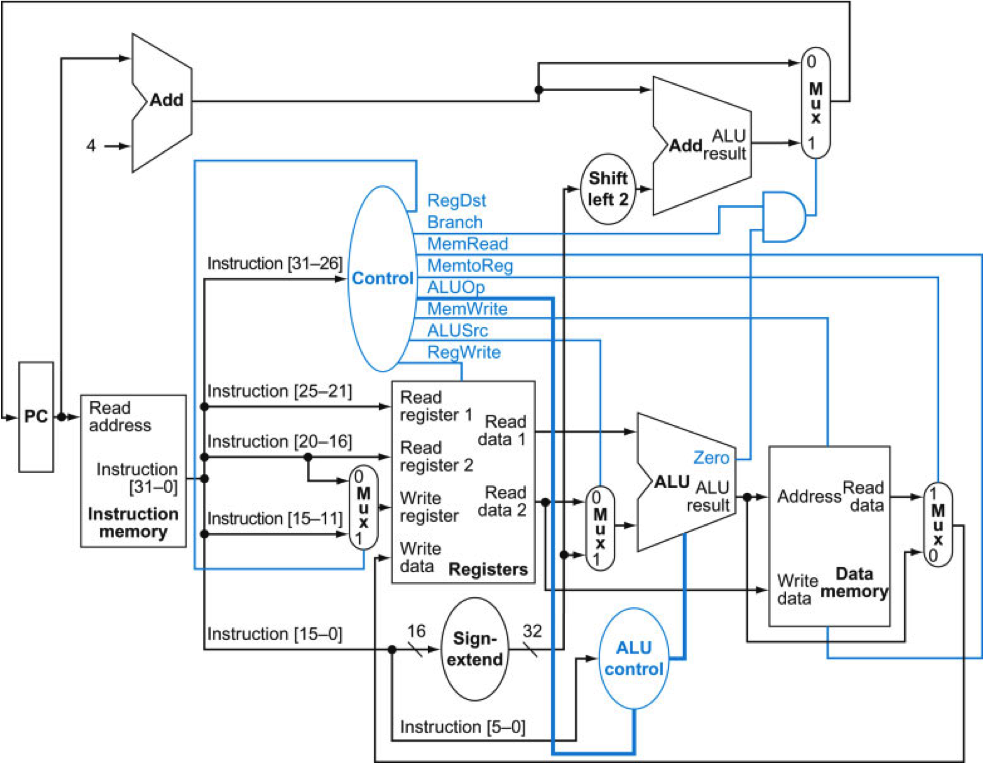
Consider our friend the datapath shown in Figure 4.17 in Patterson and Hennessy, and imagine that we're executing this instruction:
Your job is to print (or edit as a PDF or JPG or...) Figure 4.17 and show the values of as many lines on the datapath as possible. This includes control lines, lines whose values are used during this cycle, lines whose values are not used during this cycle, etc. For lines where we don't have enough knowledge of the circuitry to say, mark them as "DK" (for "don't know").
You may make the following assumptions:
Still using Figure 4.17, suppose the propagation delays of the various elements are: 12 ns for memory, 6 ns for the ALU, 4ns for the adders, 2 ns for the registers, 3 ns for the Control, 3 ns for the ALU Control, 2 ns for each of the multiplexors, 1 ns for the shift left, 1 ns for the sign extend, and 1 ns for any individual gates. Also, assume that the the PC shows the proper output immediately after the trailing clock edge.
Given these assumptions:
Hey look, we're still using Figure 4.17. This time, fill in this chart, with values for MemToReg, ALUSrc, and RegDst for each of the listed instructions:
| opcode | MemToReg | ALUSrc | RegDst | |
|---|---|---|---|---|
| lw | 100011 | |||
| sw | 101011 | |||
| beq | 000100 | |||
| add | 000000 | |||
| sub | 000000 | |||
| addi | 001000 |
Given this chart, and assuming these six instructions are the only ones you care about, draw the portion of the Control that takes the opcode as input and produces MemToReg, ALUSrc, and RegDst as output.